Results 1 to 5 of 5

Thread: Surface mount PCB with soldermask

  1. #1
    Join Date
    May 2014
    Location
    Auckland,New Zealand
    Posts
    308

    Surface mount PCB with soldermask

    I made a couple more printed circuit boards today, my first try with some surface mount components. I can now make them in about 3 hours not including artwork prep. It looks like the smallest raster gap I can do is around 0.22mm. I think a 1.5" lens and some new belts would be a good investment.

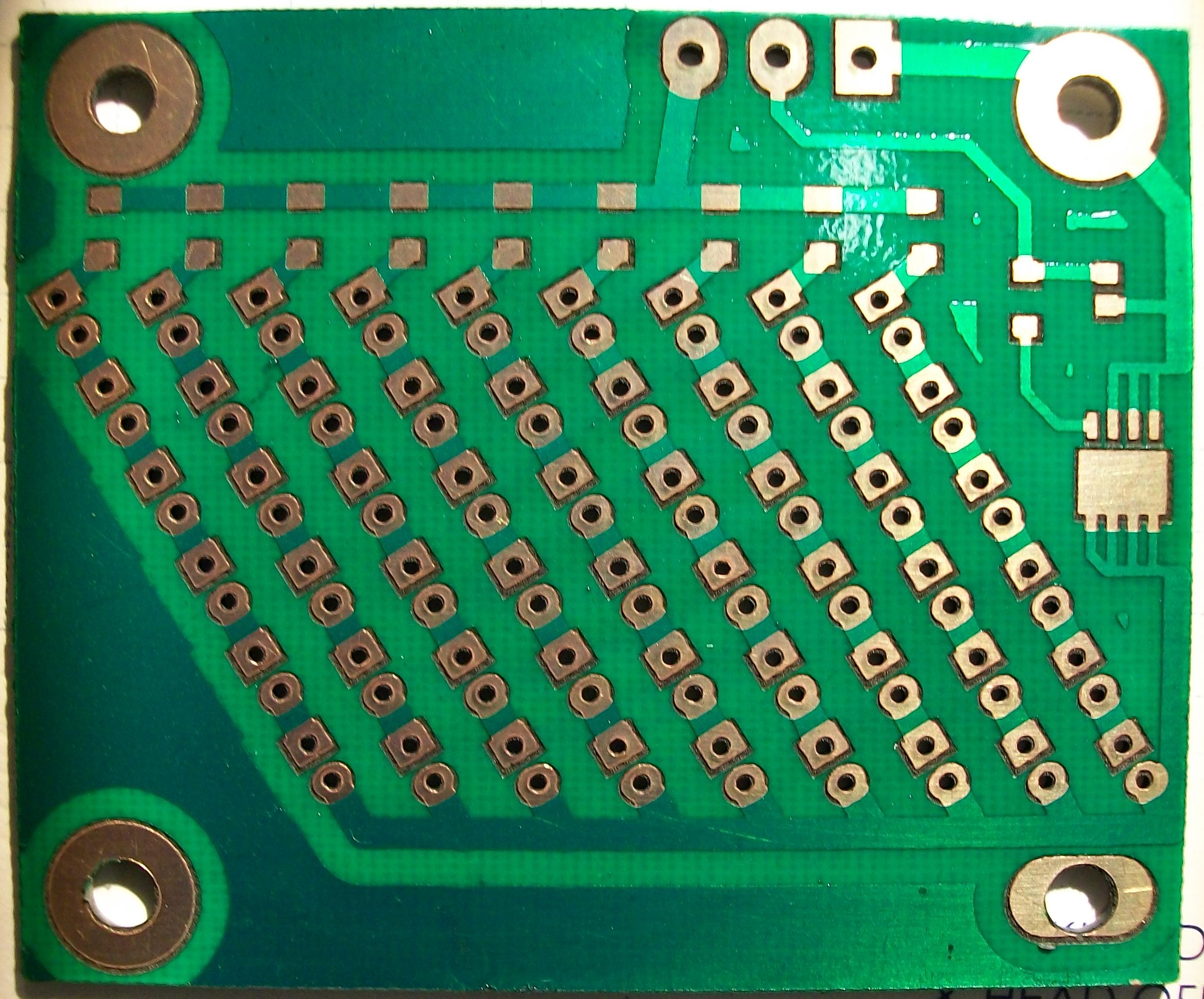
    Copper side of board


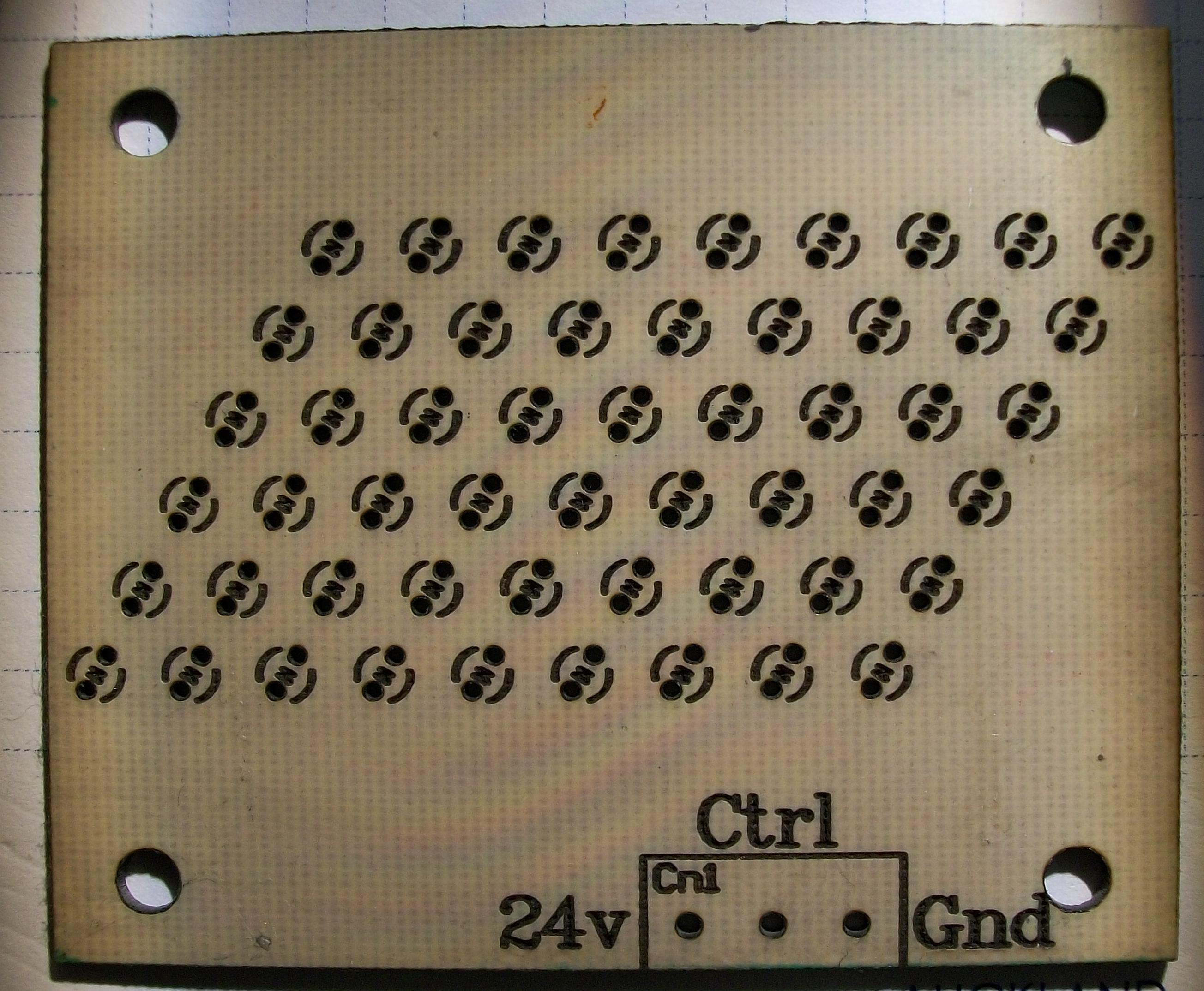
    Top side of board, laser drilled engraved and cut out


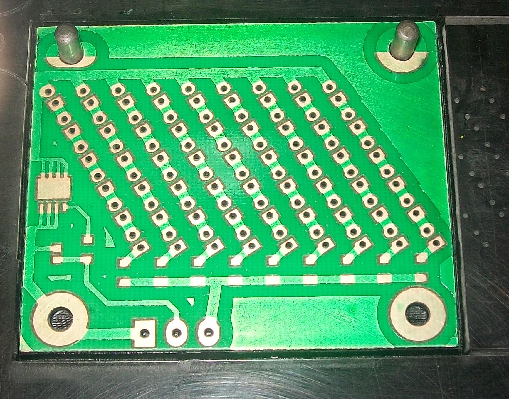
    Board on the dowel pins that are cut into 6mm acrylic on the engraving table. Note the machine is running and has not completed removing the green mask paint at the top.


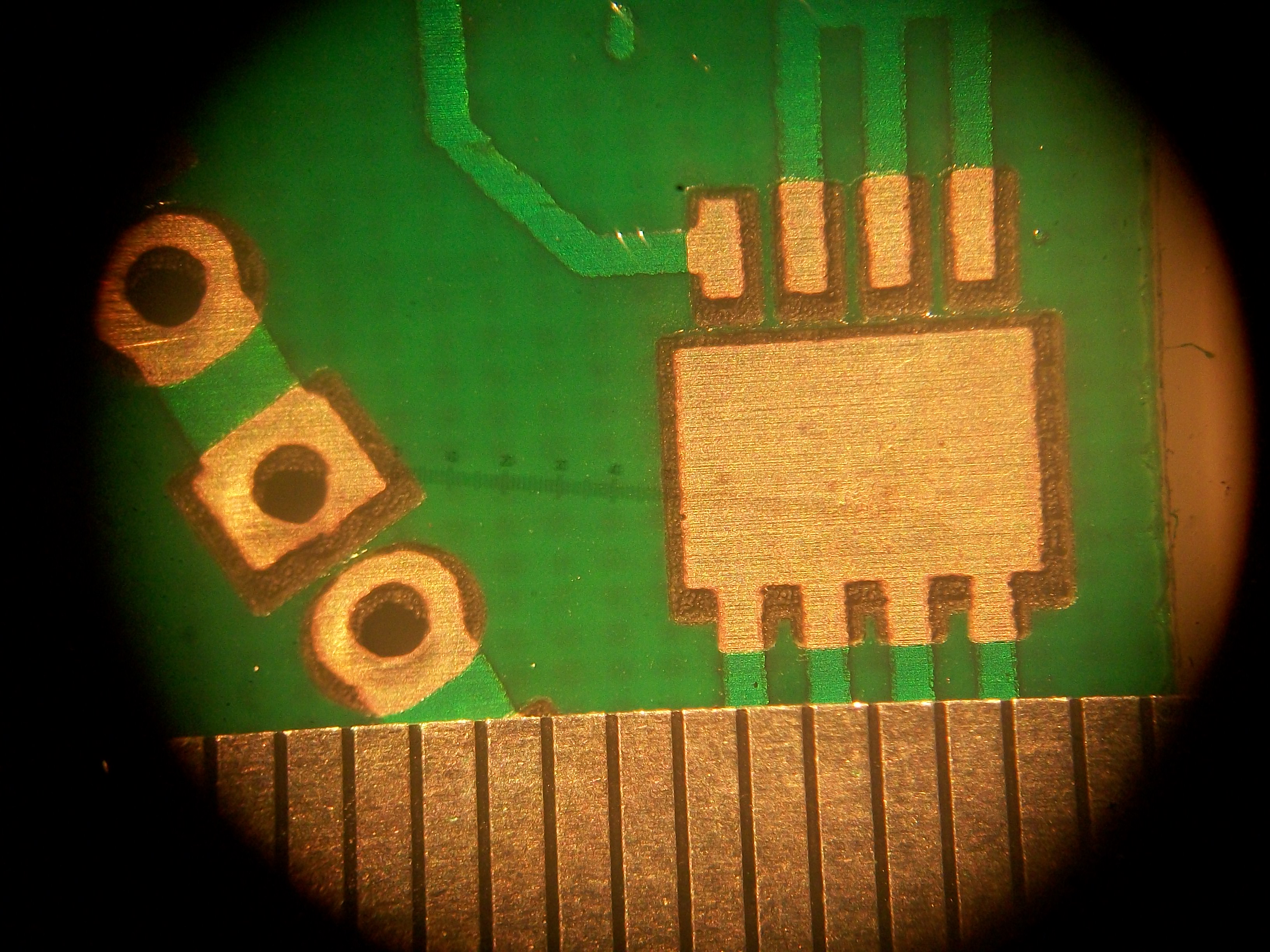
    A close up through the microscope with a mm steel rule in view.


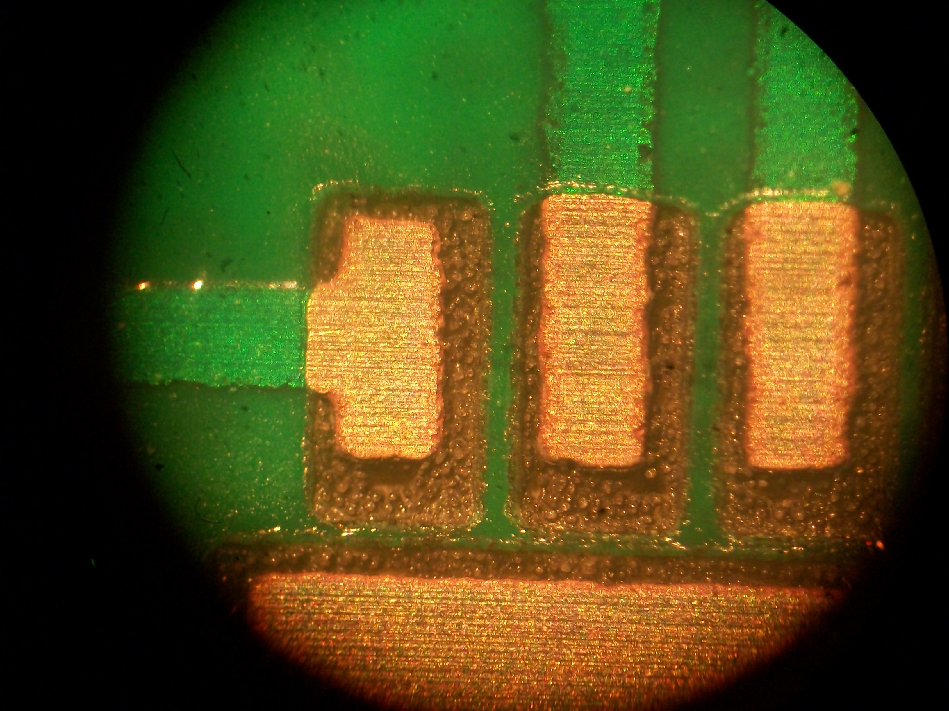
    And even closer, you can see the small misalignment I get when flipping the board.


    I have found that the carbon from the soldernask removal can leave resistance between the pins of IC's. A quick scribe between the pins fixes this but its better to avoid this in the artwork. All good fun though.
    Universal Laser VLS6.60, Tantillus 3D printer, Electronic design
    edns Group, Mairangi Bay, Auckland, New Zealand

  2. #2
    Keith - I couldn't find your previous post on this subject - can you recap as to how you are doing this and/or link to the other post? Unfortunately the search algorithm on the forum does not allow terms like "PCB" as it is "too short". I assume you are albating a resist with the laser; what resist are you using and what etching method?

    Edit

    Ok, I see now that you have a blog post so ignore my request . . . too bad the search does not work.

  3. #3
    Quote Originally Posted by Richard Rumancik View Post
    Keith - I couldn't find your previous post on this subject - can you recap as to how you are doing this and/or link to the other post? Unfortunately the search algorithm on the forum does not allow terms like "PCB" as it is "too short". I assume you are albating a resist with the laser; what resist are you using and what etching method?

    Edit

    Ok, I see now that you have a blog post so ignore my request . . . too bad the search does not work.
    Keith: Awesome!

    Richard: Forum searches are sometimes wonky for me too. Use Google and enter:

    site:www.sawmillcreek.org PCB

    https://www.google.com/search?q=site...utf-8&oe=utf-8

    Hope that helps.

  4. #4
    What type and thickness of board are you using, and how powerful of a laser? I haven't had much luck cutting holes in 1.6mm FR3 with my 60w. It has to go so slow that the copper pads get too hot and peel up. However I've only tried drilling the holes from the top after etching, rather than from the bottom beforehand. Drilling from below won't help with 2-sided boards however. I have had good luck just rastering the holes a little. That creates a divot that pulls the drill bit into position so I can get perfect placement with the drill press without spending a lot of time trying to line up the bit.

    The pins you were talking about for through holes- are they like little tubes you can stick into a hole, or are they solid pins for making vias?

  5. #5
    Join Date
    May 2014
    Location
    Auckland,New Zealand
    Posts
    308
    Hi Ian

    You can see the link to my blog here
    http://www.sawmillcreek.org/showthre...cuit-Board-Mk2

    1.6 to 1.8mm pcb cuts fine, but not through the copper of course. The holes turn to carbon and can be cleared with an air compressor after the etch. I do the non copper side first with a cut for the holes and an engrave for the component designators. My laser is in my signature. It is very focused using my microscope method.

    When I raster the copper I find I must do it twice, Once to burn the paint off and again to clean the board.

    The pins are 4mm dowel pins that are stuck to the bed with acrylic. This lets me precisely place the board for all the processes as the solder mask needs to register with the copper.

    If I did a double sided board I would laser the holes after etching. I have some little drawing pin things I got from RS that could be used for the vias. I will do a double sided board when the need arises.

    Cheers
    keith
    Universal Laser VLS6.60, Tantillus 3D printer, Electronic design
    edns Group, Mairangi Bay, Auckland, New Zealand

Posting Permissions

  • You may not post new threads
  • You may not post replies
  • You may not post attachments
  • You may not edit your posts
  •